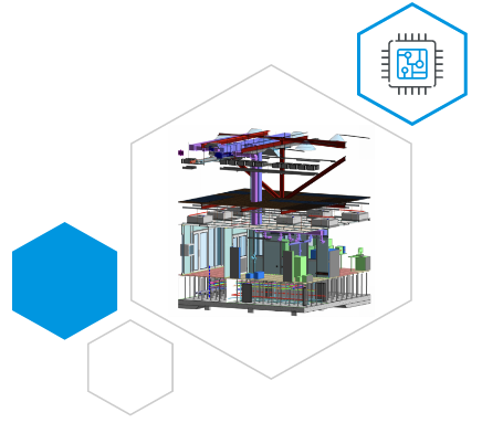
Our team of professional engineers has decades of experience in the design of thousands of square metres of fab, assembly facilities and support areas, both in the UK and internationally. Our experience in the semiconductor industry is second to none.
As manufacturing technologies populating the fab have evolved, our design solutions have developed in line with these advances. We are experienced in meeting the increasingly challenging environmental conditions required, to support the manufacture of nano-scale device geometries and the broadening spectrum of materials being used.
We have developed innovative techniques to reduce fab energy consumption. Our team has been responsible for achieving significant reduction in our clients’ operating costs and carbon footprints.
In addition to projects undertaken by AED, our team is proud to have been involved in some of the world’s largest and most technically challenging projects for leading manufacturers since the 1980s. Our experience includes Silicon, Compound Semiconductor (GaAs, InP, SiC etc), MEMS and Nano-Scale Devices.
Design & Consulting Scope:
Cleanroom
MEP (Mechanical, Electrical and Process)
Effluent and Waste Water
UPW & DI Water
Special Gases
CDA
Vibration Isolation
Tool Hook-UP
Design Experience
Our team’s design experience includes many notable projects in theUK, USA, Europe and AsiaPac including:
Intel’s first 300mm Fab. Portland Oregon
ST Microelectronics, Catania, Sicily. 12,000m2 3 level Fab.
10,000m2 Fab. Motorola. China
4,000m2 Fab. Motorola. Scotland
Nexperia. UK & Europe. Multiple fab expansion & upgrade Projects
6,000m2 Fab. Fujitsu. England
University of Southampton, Mountbatten Building. Semiconductor, Biotech, thin film, optical and MEMs research facility
Intel Fab 14. Ireland. conversion of 10,000m2 of 200mm fab to 300mm wafer production
BP Solar. Madrid. 6,000m2 silicon based PV cell manufacturing plant